FPGA Explained | Ultimate Guide to Architecture, Logic Blocks & AI
Table of Contents
INTRODUCTION TO FPGA ARCHITECTURE
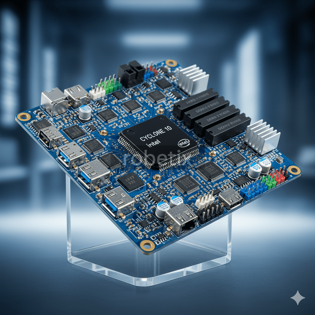
WHAT IS FPGA ? ( Field Programmable Gate Array )
(Field Programmable Gate Array) is a type of Integrated Circuit that can be changed by user itself after manufacturing to perform multiple tasks.
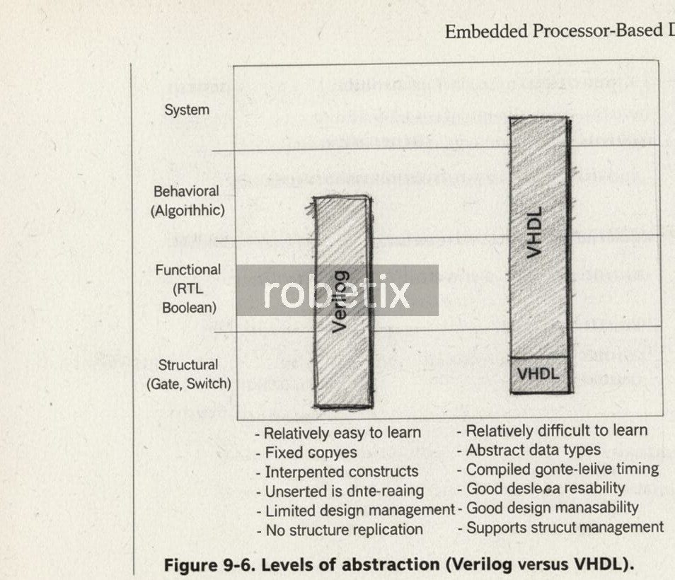
FPGA written using a language called hardware description language (HDL) that used in both FPGAs and ASICs to make changing in your device after fully manufactured that make it totally different from the other microcontroller devices. The most common HDL language for FPGAs board is Verilog just as most popular Programming language is python but a huge difference in them.
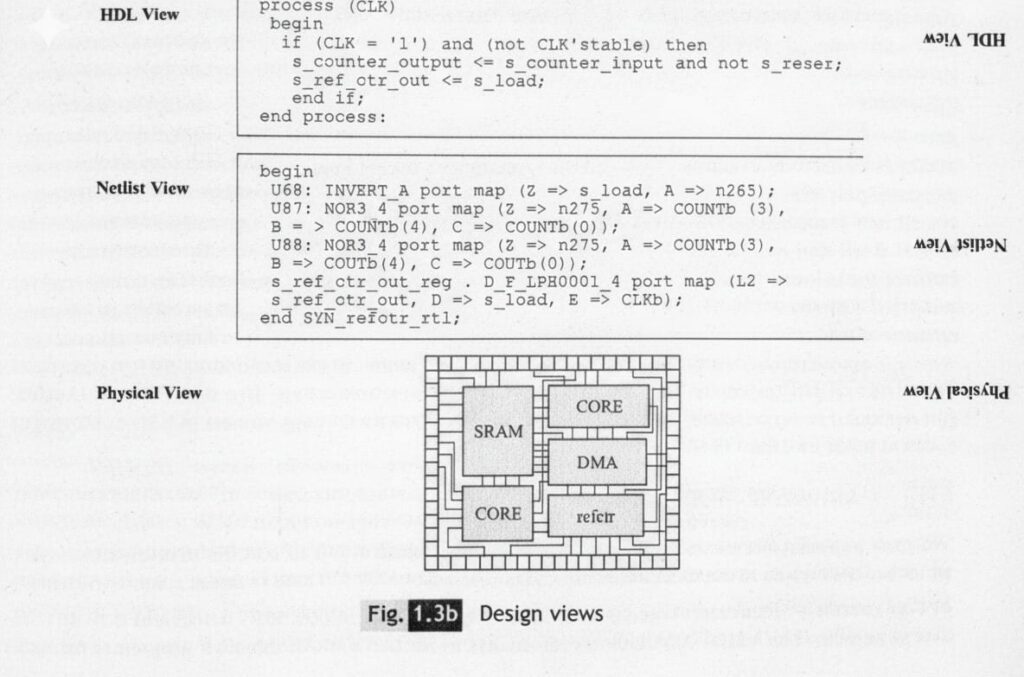
FIRST, they have circuit diagrams in which we make connections of each component, initialized their values and make a proper and professional circuit design usually called schematic.
At very early stage you have some gates to design custom low-level ICs, 1 bit and 4-bit adders and etc. and this done mostly by using two main gates NAND and NOR gate through which we implement all type of inputs and get desired output. But it’s very slower, more prone to errors and difficult to manage overall. Then as time changes you have a lot of gates and you implement them in scratch like Logisim I currently used it, and you can build from 8-bit ben eaters custom CPU up to 64-bit CPU.
The point of using gates is to replace the usage of multiple transistors in billions quantity, then we have Flip Flops that are block of memory and furthermore advancement time by time.
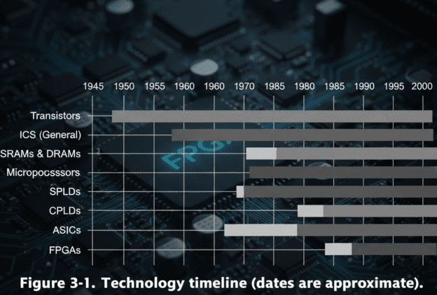
HISTORY
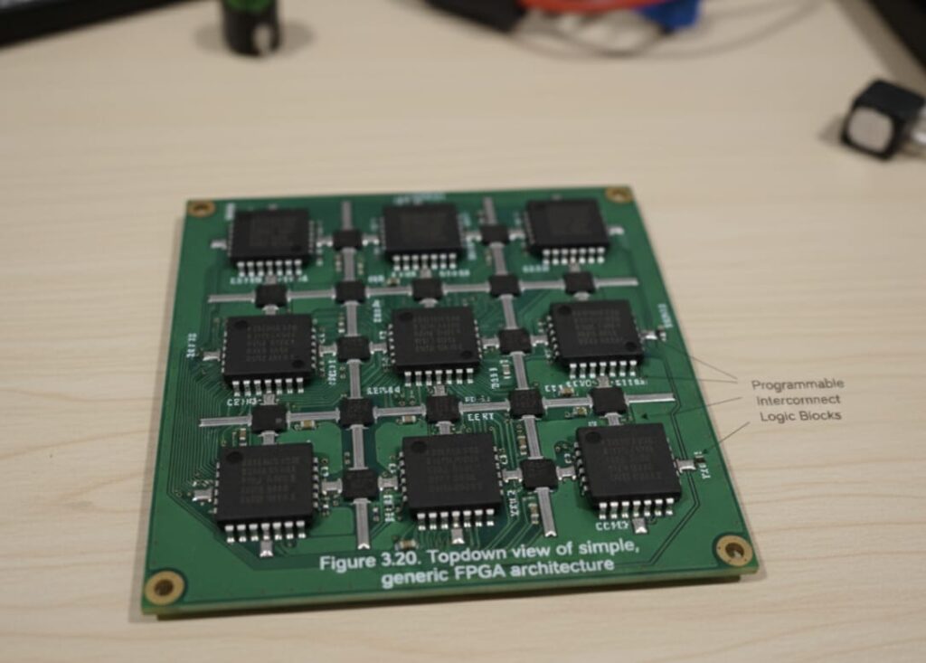
FPGAs (Field Programmable Gate Arrays) first introduced in 1985-the XC2064, it consists of multiple arrays of logic block to implement logic function in them. It has 64 configurable logic blocks (CLBs) with three main parts Routing Channel having lots of programmable wiring for data travel or routings for interconnection between logic blocks, having I/O pads at outside boundary, and Logic Block inside them which have multiple Logic Functions. In Microprocessors, you implement or write program just to fix the digital hardware but here you can program the hardware itself. It has very flexible interface to attract with like ( TTL , CMOS ).
Microsoft first use it in 2014 for Bing Search Engine due to its performance per watt and in 2018 it starts deploying these FPGAs to its other data center like Azure cloud computing.
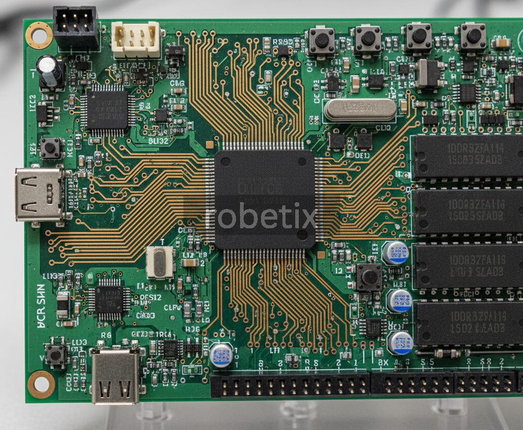
MAJOR COMPONENTS USED IN FPGAs BOARD
- CLBs (Configurable Logic Block):
These are the main building block of FPGA. They contain small logic elements like lookup tables (LUTs) and Flip-Flops that can be programmed to perform task.
- Input/Output Blocks (IOBs) or PADS:
These are FPGA connection points which control signals entering and leaving the chip, handling things like voltage level, timing and direction of I/O.
- Interconnection Wires/ Switch Matrix:
It’s the switch matrix of FPGA’s internal routing network. They connect CLBs and IOBs so signal travel between them. Linking different logic block to create a complete circuit just like buses for data transfer.
- DCM (Digital Clock Manager):
It offers flexible clocking options and management like PLLs and DLLs to generate and control clock signals within the design.
- BRAM (Block Ram / Distributed Ram):
These are the on-chip memory for data storage, FIFO buffers and other memory-based functions. The Block RAM are larger, dedicated memory blocks while Distributed RAM is spread across the CLBs.
- External Connectivity options for high-speed serial interfaces, external memory (DDR2,3 or etc.) and general purpose I/O pins (GPIO).
- HIGH SPEED Rocket IO transceivers support communication protocols like PCIe, Gigabit Ethernet and Serial Rapid IO.
HOW LOGIC BLOCK WORKS OR THINKS?
1. Calculating Logic: It is used at first step and named as LUT (LOOK UP TABLE), It takes input A, B, C and D. We can program it to acting as any logic gate (AND, NOR, XNOR or etc.) and do more complex tasks, its works is just to make logic as usually the brain does.
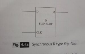
2. Remember a value: Flip-Flops basically used as a memory, and We have used here D-Flip Flop. WHY ONLY D-FLIP FLOP?? because FPGAs uses only LUT logic to calculate the output, we call it universal because every flip-flop like T, JK, SR be made using a logic before D input so it’s also simpler, faster and more efficient. Flip-Flop only gives timing and memory. It updates its value only when the clock ticks. Until the next tick, it keeps showing the same stored value. It works like If the LUT gives 1, the FF remembers that 1 until the next clock tick, even if we change input.
3. Decides What to send: The MUX decides which output to send, whether to take directly from the LUT (instant output), or from the FF (Delayed/Stored output), this choice depend on how we program the FPGA and the Programming is all inside the LUT.
Flip-flops with both “set” and “reset” inputs
Many ASIC libraries offer a wide range of flip-flops, including a selection that offer both set and reset inputs (both synchronous and asynchronous versions are usually available). By comparison, FPGA flip-flops can usually be configured with either a set input or a reset input. In this case, implementing both set and reset inputs requires the use of a LUT, so FPGA design engineers often try to work around this and come up with an alternative implementation.
CLOCKING IN FPGA
Most of FPGAs rely on synchronous system that requires clock signal, as discussed before FPGA contain routing networks for clock and reset which could be implemented through H-TREE which used to balance the clock everywhere as H-TREE splits the clock signal equally and creates a branches to get same clock in each part of FPGA, it also helps reduce time delay errors due to one clock in whole FPGA. FPGA contain analog PLL(phase-locked loop) and DLL(delay-locked loop) to synchronize different clock with different frequencies. Complex designs assign each clock section for different frequencies and phase relationship, so each forming separate clock domain.
ADVANCED FPGA FEATURES
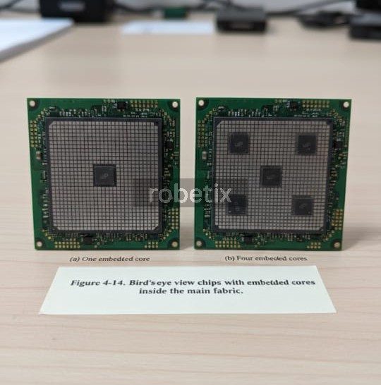
Higher end FPGAs contain high speed multi gigabit transceivers, Processor Cores, PCIe (Peripheral Component Interconnect) for attaching hardware device and Memory controller like MCC/MCU that manage flow of data going to and from a computer main memory. The Processor cores we discuss before a build using transistors instead of LUTs, so we call them ASIC-level performance, and they consume a lot of power. The Thing is some FPGAs have already built-in hardware for physical (PHY) tasks like line coding (changing data bit in special patterns for better signal integrity, regular changes for timing and error checking) while some FPGA require to implement function ourselves in logic blocks.
In 2012, it gained architectural approach of combining logic blocks and interconnect the old FPGAs with embedded microprocessor to form a complete programmable chip. One example is of Xilinx Zynq-7000 all programmable System on Chips (SoC) which include 1.0 GHz dual core ARM CORTEX-A9 embedded within FPGAs logic.
Embedded Processor Cores (hard and soft)
If the FPGA you are working multipliers, you will have to implement this function by combining the multiplier with an adder formed from a number of programmable logic blocks, while the result is stored in some associated flip-flops, in a block RAM, or in a number of distributed RAMs. Life becomes a little easier if the FPGA also provides embedded adders, and some FPGAs provide entire MACs as embedded functions.
Almost any portion of an electronic design can be realized in hardware (using logic gates and registers, etc.) or software (as instructions to be executed on a microprocessor). One of the main partitioning criteria is how fast you wish the various functions to perform their tasks:
Picosecond and nanosecond logic: This has to run insanely fast, which mandates that it be implemented in hard ware (in the FPGA fabric).
Microsecond logic: This is reasonably fast and can be implemented either in hardware or software (this type of logic is where you spend the bulk of your time deciding which way to go).
Millisecond logic: This is the logic used to implement interfaces such as reading switch positions and flashing light-emitting diodes (LEDs). It’s a pain slowing the hardware down to implement this sort of function (using huge counters to generate delays, for example). Thus, it’s often better to implement these tasks as microprocessor code (because processors give you lousy speed-compared to dedicated hardware but fantastic complexity).
The fact is that the majority of designs make use of micro-processors in one form or another. Until recently, these appeared as discrete devices on the circuit board. Of late, high-end FPGAs have become available that contain one or more embedded microprocessors, which are typically referred to as microprocessor cores. In this case, it often makes sense to move all of the tasks that used to be performed by the external microprocessor into the internal core. This provides a number of advantages, not the least being that it saves the cost of having two devices; it eliminates large numbers of tracks, pads, and pins on the circuit board; and it makes the board smaller and lighter.
Hard VS Soft Cores
- Hard cores:
A hard microprocessor core is one that is implemented as a dedicated, predefined (hardwired) block (these cores are only available in certain device families). Each of the main FPGA vendors has opted for a particular processor type to implement its hard cores. For example, Altera offer embedded ARM processors, QuickLogic have opted for MIPS-based solutions, and Xilinx sports PowerPC cores. Of course, each vendor will be delighted to explain at great length why its implementation is far superior to any of the others (the problem of deciding which one actually is better is only compounded by the fact that different processors may be better suited to different tasks).
In this scenario, all of the components are typically formed on the same silicon chip, although they could also be formed on two chips and packaged as a multichip module (MCM).One advantage of this implementation is that the main FPGA fabric is identical for devices with and without the embedded microprocessor core, which can make things easier for the design tools used by the engineers. The other advantage is that the FPGA vendor can bundle a whole load of additional functions in the strip to complement the micro-processor core, such as memory and special peripherals.
In this case, the design tools have to be able to take account of the presence of these blocks in the fabric; any memory used by the core is formed from embedded RAM blocks, and any peripheral functions are formed from groups of this scheme can argue that there are inherent speed advan general-purpose programmable logic blocks. Proponents of this scheme can argue that there is inherent speed.
- Soft microprocessor cores:
As opposed to embedding a microprocessor physically into the fabric of the chip, it is possible to configure a group of programmable logic blocks to act as a microprocessor. These are typically called “soft cores,” but they may be more precisely categorized as either soft or firm, depending on the way in which the microprocessor’s functionality is mapped onto the logic blocks. For example, if the core is provided in the form of an RTL netlist that will be synthesized with the other logic, then this truly is a soft implementation. Alternatively, if the core is presented in the form of a placed and routed block of LUTs/CLBs, then this would typically be considered a firm implementation.
In both of these cases, all of the peripheral devices like counter timers, interrupt controllers, memory controllers, communications functions, and so forth are also implemented as soft or firm cores (the FPGA vendors are typically able to supply a large library of such cores). Soft simpler than their cores are slower and hard-core counterparts (of course they are still incredibly fast in human terms). However, in addition to being practically free, they also have the advantages that you only have to implement a core if you need it and that you can instantiate as many cores as you require until you run out of resources in the form of programmable logic blocks.
One cool thing about the integrated development environment (IDE) fielded by Xilinx is that it treats the PowerPC hard core and the Micro Blaze soft core identically. This includes both processors being based on the same Core Connect processor bus and sharing common soft peripheral IP cores. All of this makes it relatively easy to migrate from one processor to the other.
Also of interest is the fact that Xilinx offers a small 8-bit soft core called the Pico Blaze, which can be implemented using only 150 logic cells (give or take a handful). By com parison, the Micro Blaze requires around 1,000 logic cells.
3D ARCHITECTURE IN FPGA
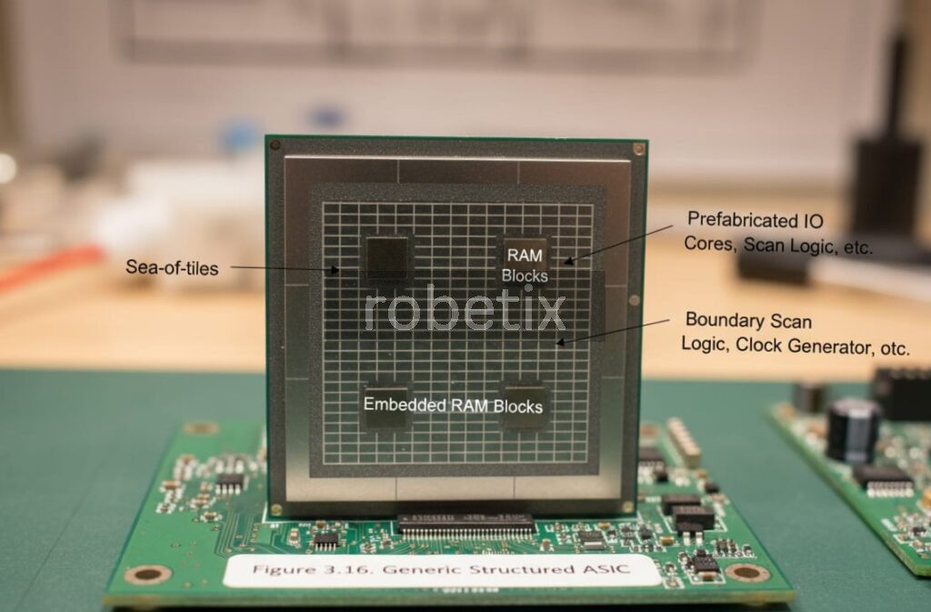
FPGAs are used to made one big chip/one dies, but big chips are too expensive, harder to manufacture and uses more power so now companies like Xilinx’s and Altera’s (Intel) use a 3D ARCHITECTURE method so they combine multiple smaller chips inside one single package, so these dies are connected internally by special silicon layer.
In this Xilinx’s takes 3 to 4 small FPGA dies and place them side by side on thin silicon layer that connects them, this way each die use different manufacture technology like one uses FPGA logic , one for high speed transceivers and another for memory so that’s how it made of different types of chips just by combining them all in single package.
Intel Directly uses EMIB (Embedded Multi-die Interconnect Bridge) a small silicon bridge inside the package that connects different dies together having same goal to connect logic die, memory die, and transceiver die efficiently.
How FPGA vendors design their chips
Last but not least, one question that is commonly asked but is rarely (if ever) addressed in books on ing a new generation of devices? FPGAs is, how do FPGA vendors actually go about designing a new generation of devices?
To put this another way, do they handcraft each transistor and track using a design flow similar to that of a full-custom ASIC, or do they create an RTL description, synthesize it into a gate-level netlist, and then use place-and-route software along the lines of a classic ASIC (gate array or standard cell) design flow.
The short answer is yes! The slightly longer answer is that there are some portions of the device, like the programmable logic blocks and the basic routing structure, where the FPGA vendors fight tooth and nail for every square micron and every fraction of a nanosecond. These sections of the design are handcrafted at the transistor and track level using full-custom ASIC techniques. On the bright side, these portions of the design are both relatively small and highly repetitive, so once created they are replicated thousands of times across the face of the chip.
Then there are housekeeping portions of the device, such as the configuration control circuitry, that only occur once per device and are not particularly size or performance critical These sections of the design are created using standard cell ASIC-style techniques.
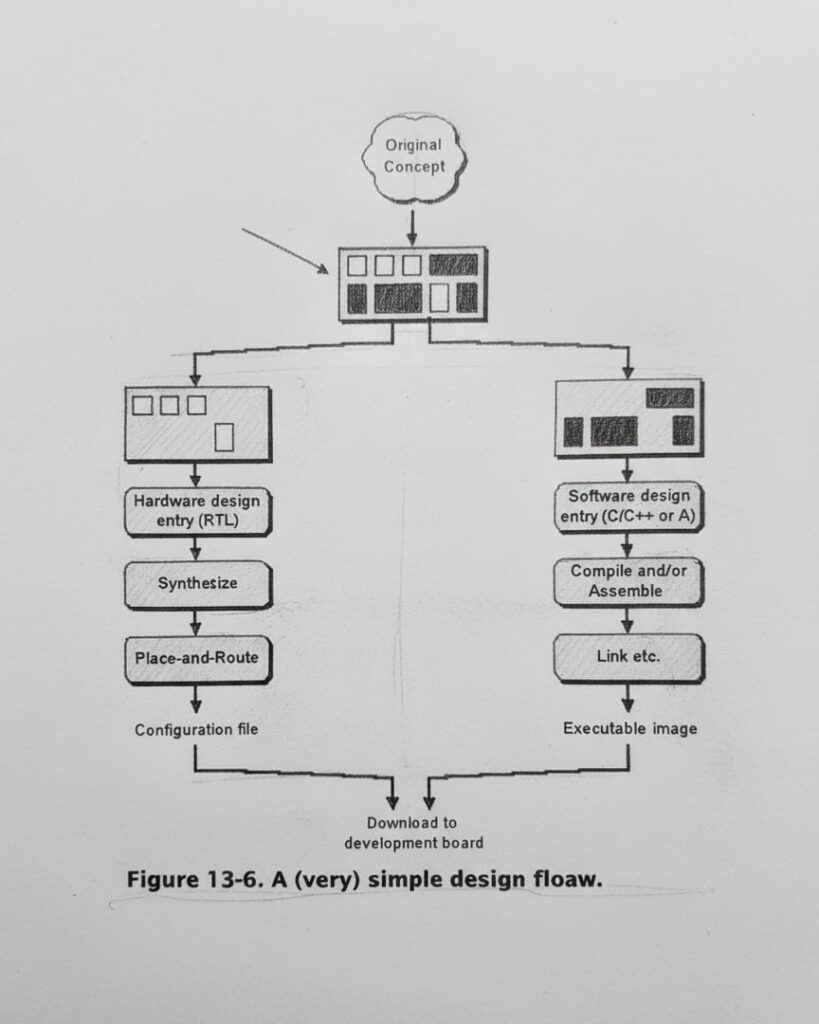
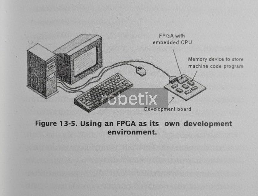
Using an FPGA as its own development environment
Perhaps the simplest place to start is the scenario where the FPGA is used as its own development environment. The idea here is that you have an SRAM-based FPGA with an embedded processor (hard or soft) mounted on a development board that’s connected to your computer. In addition to the FPGA, this development board will also have a memory device that will be used to store the software programs that are to be in by the embedded CPU.
Once the system architects determined which portions of the design are to be implemented in hardware and software, the hardware engineers start to capture their RTL blocks and functions and synthesize them down to a LUT/CLB-level netlist. Meanwhile, the software engineers start to capture their C/C++ programs and routines and compile them down to machine code. Eventually, the LUT/CLB-level netlist will be loaded into the FPGA via a configuration file, the linked machine code image will be loaded into the memory device, and then you let the system run wild and free (Figure 13-6).
FPGA MARKET IMPACT AND APPLICATION
FPGAs are currently eating into four major market segments: ASIC and custom silicon, DSP, embedded microcontroller applications, and physical layer communication chips. Furthermore, FPGAs have created a new market in their own right: reconfigurable computing (RC).
ASIC and custom silicon:
Today’s FPGAs are increasingly being used to implement a variety of designs that could previously have been realized using only ASICs and custom silicon.
Digital signal processing:
High-speed DSP has traditionally been implemented using specially tailored microprocessors called digital signal processors (DSPs). However, today’s FPGAs can contain embedded multi-pliers, dedicated arithmetic routing, and large amounts of on-chip RAM, all of which facilitate DSP operations. When these features are coupled with the massive par-allelism provided by FPGAs, the result is to outperform the fastest DSP chips by a factor of 500 or more.
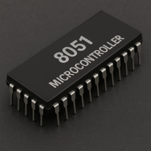
Embedded microcontrollers:
Small control functions have traditionally been handled by special-purpose embedded processors called microcontrollers. These low-cost devices contain on-chip program and instruction memories, timers, and I/O peripherals wrapped around a processor core. FPGA prices are falling, however, and even the smallest devices now have more than enough capability to implement a soft processor core combined with a selection of custom I/O functions. The end result is that FPGAs are becoming increasingly attractive for embedded control applications.
Physical layer communications:
FPGAs have long been used to implement the glue logic that interfaces between physical layer communication chips and high-level networking protocol layers. The fact that today’s high-end FPGAs can contain multiple high-speed transceivers means that communications and networking functions, which once required separate chips, can be integrated directly onto the FPGA itself.
FUTURE AND AI
As of 2018, The Increase in AI application will also affect of hardware accelerated acceleration for this they use AI accelerators including Microsoft Catapult and for accelerating ANN (Artificial Neural Network) and Machine Learning application. One of best use of FPGA is that by time changes and arrival of new technology you don’t need to be stuck and panic and dependent on the previous version of FPGAs, just changes the logic implement some reasoning in it and there you go.
Drop your thoughts below, even one-word counts!
Take Care Goodbye 🙂
Frequently Asked Questions
An FPGA is a reconfigurable Integrated Circuit that allows users to program and modify its hardware logic after manufacturing. Unlike microcontrollers, that execute predefined instructions, FPGAs let you design custom digital circuit directly in hardware using HDL such as Verilog or VHDL.
A modern FPGA consist of Configurable Logic Blocks (CLBs), Input/Output Blocks (IOBs), Interconnection networks (switch matrix), Digital Clock Manager (DCM) and Block Ram (BRAM).
FPGAs are increasingly used in AI acceleration, particularly in deep learning, neural networks and Edge AI systems. Their reconfigurable logic enables faster interface, parallel computation and lower power consumption compared to traditional CPUs and GPUs.
A hardcore is a Fixed, pre-implemented processor (like ARM Cortex A9) built into the FPGA silicon for high-speed performance. Softcore such as Xilinx Micro Blaze or Altera is implemented using FPGA logic blocks, providing flexibility to modify multiple processors depending on project need.

SHARE WITH YOUR FRIENDS